
TM 9-6625-1753-14
same way as the difference amplifier described in paragraph 3-12d (trigger generation). Each of these circuits employs a
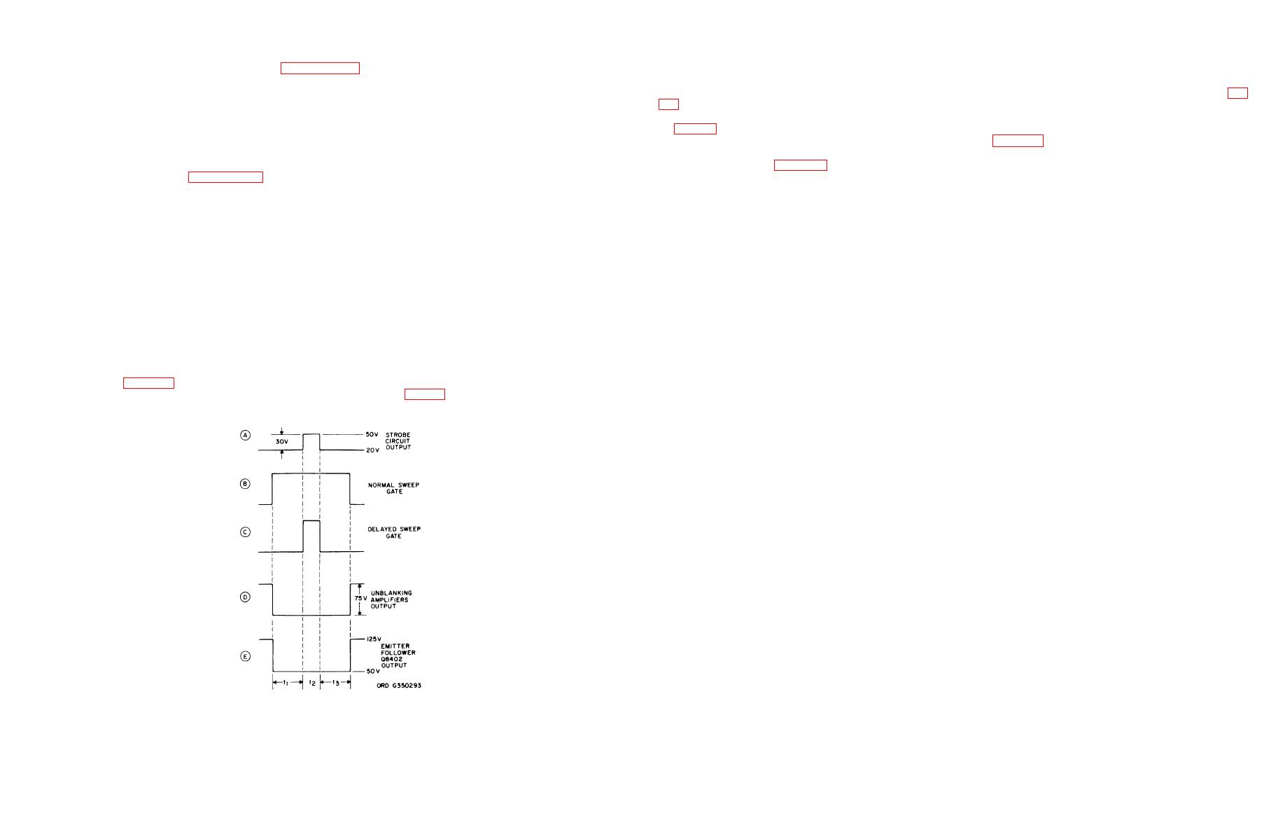
applied to it.) STROBE ADJ resistor R8012 controls the dc level of the strobe circuit output.
tunnel diode to produce a squared pulse output. Although a sawtooth signal is used instead of a sine wave, it doesn't alter the
operation of the circuit.
(8) The positive gates from the normal-sweep gate multivibrator and delayed-sweep gate multivibrator (B and C, fig.
3-8) are applied to unblanking (cascode) amplifiers Q8404 and Q8405 (zones C13, C14). The outputs of these two amplifiers
(4) Amplifier Q8604, resistor R8621, and capacitor C8611 differentiate the square-wave output of the comparator
are combined, and applied to unblanking amplifier Q8403. The resultant negative-going output of the unblanking amplifiers,
circuit, and apply it to transformer T8601. Because of the transformer winding configuration, you will notice that the positive
(D, fig. 3-8) having an overall 75-volt amplitude, is applied to emitter follower Q8402. The output from emitter follower Q8402
pulse, representing the leading edge of the comparator circuit output, when applied to diode CR8105, becomes a negative
is applied to the beam gate plate (pin 6) and is shown by waveform E of figure 3-8.
pulse. Passing through the diode, the negative pulse triggers delayed-sweep gate multivibrator Q8106, Q8107. The negative
gate output of the delayed-sweep gate multivibrator activates the sawtooth generating circuit (V8103, V8104), which is
(9) Referring to figure 3-8, you see that during the interval represented by t1, 50 volts is applied to the beam gate
identical to the one described in paragraph 3-13a through d.
plate (pin 6). The other beam gate plate (pin 13) receives the output of strobe circuit, which during this interval generates a
constant voltage (approximately 20 volts) because the delayed-sweep gate multivibrator hasn't been activated yet. Now the
(5) Before continuing with this description, let's cover the method of balancing both the normal- and delayed- sweep
potential difference between the plates (approximately 30 volts) is such, that the electron beam is deflected by an amount that
circuits to produce identical sweep rates. Notice that the negative gates from the normal- and delayed- sweep gate
allows only a portion of it to pass through the aperture of the shield. This reduces the brightness of the CRT display.
multivibrators, that remove the clamping voltage from the grids of the Miller integrators via the reverse-biased disconnect
diodes, also remove the clamping voltage from the Miller integrator cathodes by reverse-biasing diodes CR8213 and CR8109
(10) During the interval represented by t2, both deflection plates receive approximately the same potential (50 volts). It
(zones A10 and D10). With both sweep circuits activated, SWP RATE BAL resistor R8175 (connecting both Miller integrator
is during this interval that the delayed-sweep gate multivibrator is activated, causing the strobe circuit to produce a positive
cathode circuits) (zone C11) is adjusted so the conduction through the tubes (V8203, V8103) is approximately the same. You
gate. With both beam gate plates at the same potential, the entire electron beam passes through the aperture, producing a
make this adjustment so that both the normal and delayed sweep circuits produce the same sweep rates at identical settings
brighter CRT display.
of the TIME/DIV switch.
(11) Upon completion of interval t2, the delayed sweep gate multivibrator is deactivated. At the same time, the strobe
(6) Continuing with the description of the triggered-strobe mode, notice that only the normal sawtooth generator
circuit goes back to its initial operating state, producing a constant output (approximately 20 volts). Thus, we see that the
output goes to the horizontal deflection amplifier circuit. In order to obtain the strobe effect, a portion of the displayed signal
potentials applied to the beam gate plates during the intervals represented by t1 and t3 are the same. This results in a dimmer
must appear narrower, and brighter. This is accomplished by setting the DELAYED SWEEP TIME DIV switch to a shorter
CRT display.
time period than the setting on the normal sweep TIME/DIV switch.
(12) Paragraphs (9) through (11) above described conditions where it is assumed the delayed sweep ends some time
(7) The positive gate output of the delayed-sweep gate multivibrator goes to strobe circuit Q8001, Q8002 and to the
during the normal sweep interval. However, suppose you adjust the DELAY VERNIER control so that the delayed sweep
beam gate circuit (par. 3-13f). Amplifier Q8001 (zone C14) inverts the positive gate and applies it to the amplifier Q8002.
starts near the end of the normal sweep. Let's further assume that the duration of the delayed sweep extends beyond the end
Here, the gate is amplified and again inverted. The resultant positive gate (A, fig. 3-8), having a 30-volt amplitude, is applied
of the normal sweep. Under these conditions, the retrace of the normal sweep would be displayed and appear bright; this is
to the beam gate plate (pin 13). (During the normal sweep mode this beam gate plate had a constant 50-volt potential
undesirable. To prevent this from happening, the positive-gate output of the normal-sweep gate multivibrator is used to return
the delayed-sweep gate multivibrator to its initial operating state.
(13) The positive-gate output of the normal-sweep gate multivibrator (Q8206) is differentiated by RC network C8126,
R8157 (zone C9), resulting in positive and negative pulses that are applied to diode CR8107. The diode allows only the
negative pulse, representing the trailing edge of the gate, to pass, triggering the delayed-sweep gate multivibrator. Returning
to its initial operating state, the delayed-sweep gate multivibrator output deactivates the delayed sawtooth generator, cutting
off the delayed sweep. At the same time, the strobe circuit produces a constant output (approximately 20 volts). With the
output of emitter follower Q8402 (a level of 125 volts) and the constant output of the strobe circuit applied to the beam gate
plates, there is more than the required 75- volt potential difference to prevent the electron beam from passing through the
aperture on the shield.
(14) An effect may appear where the bright segment (strobe), instead of being coincident with the trace on the CRT
Figure 3-8. Beam gate plate input waveforms (triggered-strobe mode).
3-11

