Home
Download PDF
Order CD-ROM
Order in Print
Figure 4. RF Input, Attenuator Control and 120 MHz Low Pass Filter, Schematic Diagram (replacement for Service Sheet 3 in 8553B Operating and Service Manual)
Figure 6. 1 MHz Crystal Oscillator, Frequency Divider and APC Compensation Circuits, Schematic Diagram (replacement for Service Sheet 7 in 8553B Operating and Service Manual)
TM-11-6625-2781-14-P-2 - index
Page Navigation
214
215
216
217
218
219
220
221
222
TM
11-6625-2781-14&P-2
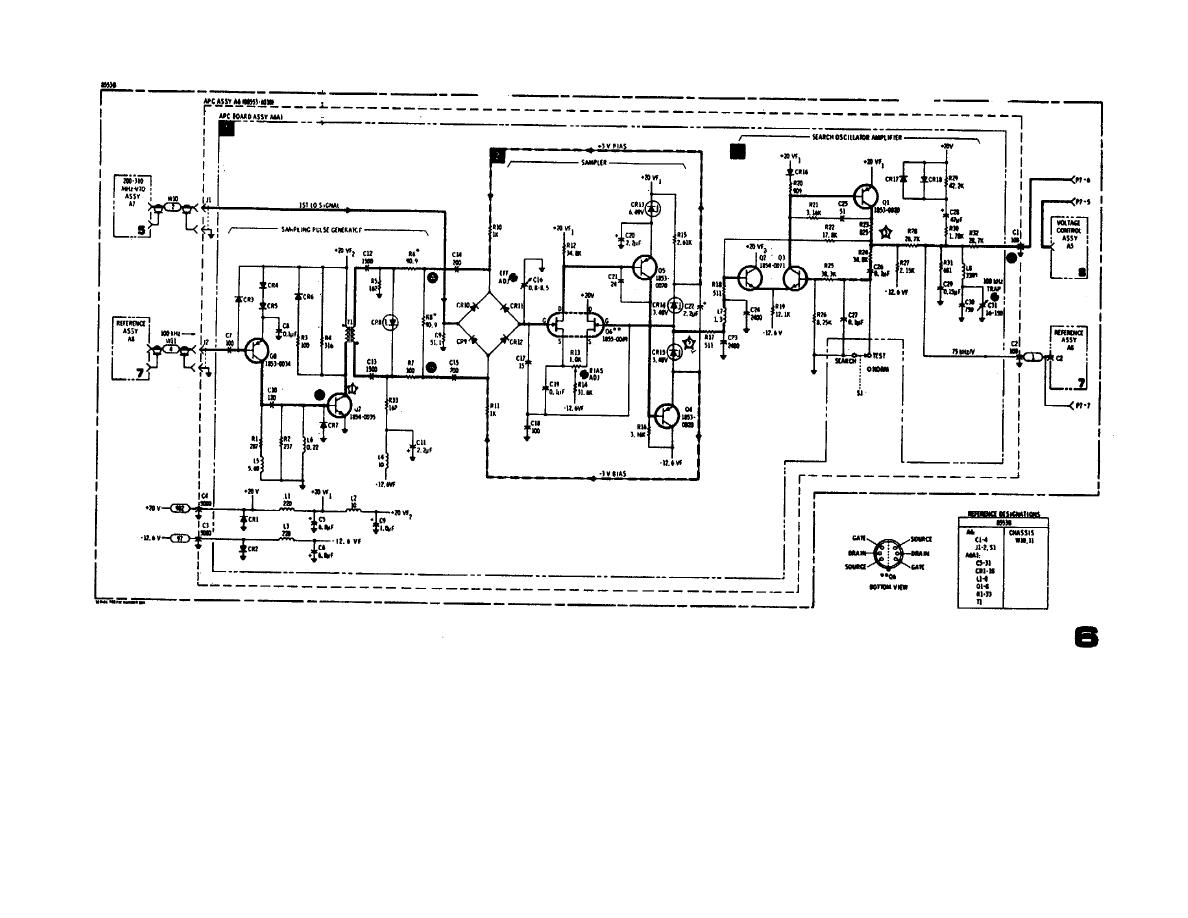
Figure
5.
Automatic
Phase
Control
and
Sampler/Amplifier
Circuits,
Schematic
Diagram
(replacement
for
Service
Sheet
6 in
8553B
Operating
and
Service
Manual)
E-7