TM 11-6625-2781-14&P-2
Switch wafer S1-3R controls the automatic phase
operate diode switching matrixes in the IF section LC
Switch wafers S1-2F, S1-1R, S1-2R, and part of S2-5R
SERVICE SHEET 2 (1 of 3)
compensation circuit (Service Sheet 8).
provides a variable voltage divider which attenuates the
Filter and Crystal Filter circuits to switch components in or
out of the circuits to control the bandwidth. It also
scan ramp voltage to determine the scan width per
SWITCHING INFORMATION (General)
Part of switch wafer S2-5F works in conjunction with the
division (Service Sheet 9 ).
provides a dc level to operate bypass paths in the Crystal
BANDWIDTH switch (Service Sheet 11).
Filter circuits when bandwidths of 10 kHz or greater are
Unless otherwise noted, all switches shown in this manual
Part of switch wafers S2-5F and S2-5R (Service Sheets 2
chosen.
are shown in the full composition.
For information
Switch wafers S1-4F and S1-4R provides current to the
and 8) provide coupling between the RF section summing
concerning switch symbols used, see Paragraphs 8-53
analogic circuit to aid in illuminating the DISPLAY UNCAL
amplifier, shaping amplifier, RF section marker generator,
A separate wafer of the switch provides current to a
through 8-58.
light when analyzer control settings are not compatible
and/or the preset scan assembly depending on the
summing bus for the analogic circuit.
with calibrated operation.
selected mode of operation.
The bandwidth switch assembly provides dc levels to
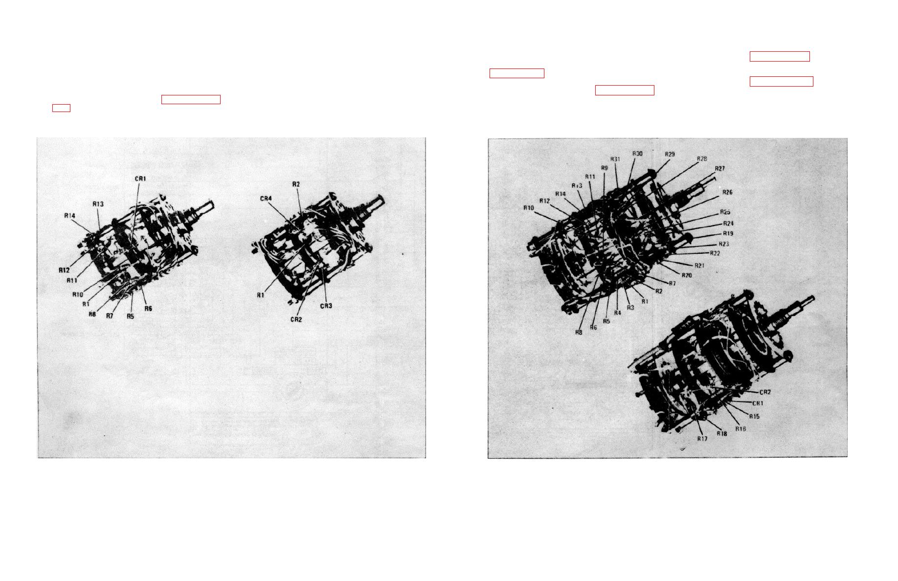
Figure 8-20. Bandwidth Switch Assembly A1 (08553-60126)
Figure 8-21. Scan Width Attenuator Assembly A2 (08553-60125)
SERVICE SHEET 1
Block Diagram
8-24


