
TM 11-6625-2781-14&P-2
Section VIII
5 AUTOMATIC PHASE COMPENSATION ASSY
SERVICE SHEET 1
BLOCK DIAGRAM
The 100 kHz reference signal controls a sampling pulse
generator which turns on a diode quad gate to sample
1 INPUT CAPACITOR ASSEMBLY A12
the output of the first local oscillator. After phase lock
has been accomplished this signal sample is used to
Input blocking capacitor A12C1 protects the diodes in
provide an error signal to maintain the phase locked
the first balanced mixer when a signal containing dc
50
condition. The APC assembly also provides an output
components is applied to the analyzer.
MHz
signal which is used to produce an offset signal to shift
IF TO
the IF Section 47 MHz oscillator frequency and maintain
8552
2 INPUT ATTENUATOR AND LOW PASS FILTER
display accuracy.
The input attenuator contains three fixed, pad type
6 REFERENCE ASSEMBLY
attenuators of 10, 20 and 30 dB. Switch positions select
one or two of the pads or straight through wiring in six
The 100 kHz reference signal is developed in the
different combinations, to provide 0 to 50 dB attenuation
reference assembly from a 1 MHz crystal controlled
in 10 dB steps.
oscillator by means of divide-by-five and divide-by-two
circuits. The reference signal provides a means of
Ganged with the input attenuator, but not a part of the
phase locking the first local oscillator to a stable
input attenuation circuit, is a wafer which provides power
reference.
to the index lamps associated with the LOG REF LEVEL
LINEAR SENSITIVITY control. This wafer also provides
The memory amplifier provides the offset voltage to
a control to the IF section log/lin amplifier which is used
shift the IF section 47 MHz oscillator an amount equal to
when the analyzer is operated in the LINEAR mode.
the frequency shift required t phase lock the first local
The Low Pass Filter response is essentially flat up to
oscillator. This is necessary to prevent CRT display
110 MHz. Attenuation at 130 MHz is approximately 3
shift when the analyzer is operated in the stabilized
dB and maximum signal rejection is between 400 and
mode.
510 MHz.
7 VOLTAGE CONTROL ASSY CIRCUITS
3 200 MHz IF ASSEMBLY
The first local oscillator summing amplifier combines the
The first mixer is a double balanced diode quad that up-
ramp voltage from the SCAN WIDTH switch, the APC
converts the input rf signals by mixing them with the
signal, and the dc level established by the position of
output of the first local oscillator. The resulting 200 MHz
the FREQUENCY control. In ZERO and PER DIVISION
IF signals are amplified 14 dB and applied to the second
modes of operation this composite signal is applied to
converter through a 200 MHz + 2 MHz filter.
the first local oscillator shaping circuit for processing. In
the 0 to 100 MHz mode, the DC tune voltage is applied
4 200-310 MHz VOLTAGE TUNED OSCILLATOR
to the marker generator.
The main frequency determining element in the first
The first local oscillator shaping amplifier shapes the
local oscillator is a varactor which is controlled by a dc
sweep tuning ramp. As the sweep voltage increases,
level or a varying ramp from the voltage control
diodes sequentially turn on parallel resistive networks to
assembly.
The VTO assembly contains a power
control the gain of the shaping, amplifier. The shaping
amplifier and separate buffer stages to provide an
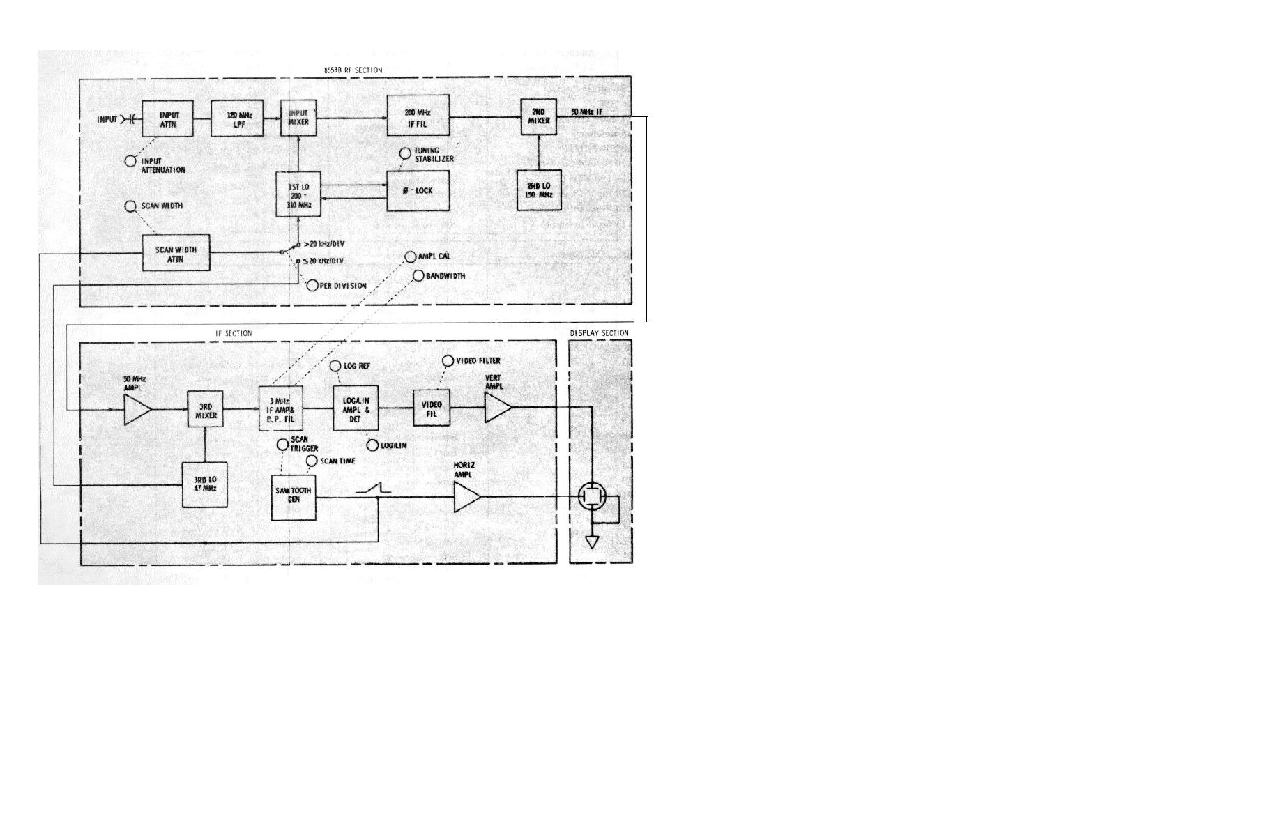
Simplified Analyzer Block Diagram
amplifier output is exponential ramp which changes the
output to the first mixer, the Automatic Phase
varactor capacity in the first local oscillator to produce
Compensation circuit, and a rear panel monitor
linear frequency change with respect to time.
connector.
8 FREQUENCY RANGE ASSEMBLY
The first local oscillator may be swept through its entire
operational range or selected portions of it, by a voltage
Controls the tuning range of the FREQUENCY control.
ramp from the voltage control assembly. In narrow scan
Divides DC tune voltage by 10 to provide 0-11 MHz
modes or in ZERO scan mode the first local oscillator is
frequency scale.
phase locked to the 100 kHz reference signal.
8553B ASSEMBLY AND ADJUSTMENT LOCATIONS
8-22
