
TM
11-6625-255-14/TO
33A1-13170-1
grid variations to ground. The output of V12 is
capacitances, t h e r e f o r e , it consumes a smaller
passed to V13 through C29. Resistor R75 is a grid
part of the available tube output voltage, and the
limiting resistor.
output voltage developed across the cathode
b. Tube V13 is the output voltage amplifier of
resistance rises. T h i s rise in high-frequency
the vtvm circuit. Grid bias for V13 is obtained
response approximately offsets the drop in high-
from the negative bias supply through R66.
frequency response caused by shunt capacitances
R e s i s t o r R68 is the plate load, and R69 is the
in the input and output circuits. The output of the
screen grid voltage dropping resistor. The parallel
voltage divider circuit is passed to the grid of V12
combination of C28C and C28D (C38B) bypasses
t h r o u g h C26.
the screen grid to ground. The output of V13 is
6-8. Voltage Amplifier and Meter Circuit
passed through C30 and applied to the plate of
V14A (CR2, TD-723D/U only) through R73 and
to the cathode of V14B (CR1, TD-723D/U only)
gram of the voltage amplifier and meter circuit.
through R74. The output of V13 is also connected
Tube V12 is the first voltage amplifier of the vtvm
t o OSCILLOSCOPE binding post E11.
circuit. Grid bias for V12 is obtained from the
c. Tube V14 (CR1 and CR2 of TS-723D/U) is a
negative bias supply through R59. Resistor R64 is
full-wave rectifier which converts the ac voltage
the plate load for V12. Resistor R65 is the screen
output of V 13 to direct current for operation of
grid voltage dropping resistor. The parallel com-
meter M1. Tube V14B (CR1 of TS-723D/U) pro-
bination of C28A and C28B bypasses the screen
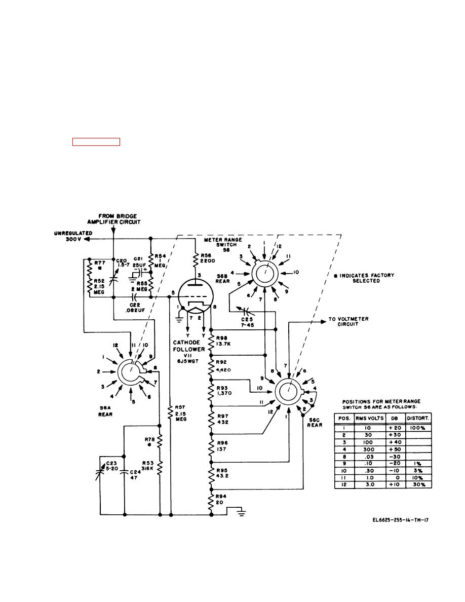
simplified schematic diagram,
Figure 6-9. Voltage divider circuit,
Spectrum Analyzer TS-723B/U, TS-723/U, and
TS-723D/U.
6-9
