
TM 11-6625-2781-14&P-2
provides the input to the mixer buffer stage through center
The output of the power amplifier is coupled through center
tapped transformer T1. Common emitter amplifier Q6provides
tapped transformer T3 and center tapped transformer T2 to
a 1V rms (typical) signal to drive the double balanced bridge
the buffer amplifiers. T'2 and T3 are not inductively coupled.
mixer in the 200 MHz IF assembly.
TEST PROCEDURE
TEST PROCEDURE
With the analyzer operating in ZERO scan mode and tuned to
Connect the output of the HP 608F (any frequency between
0 MHz, check for the presence of typical signal levels
200-310 MHz) to the Q4 collector side of T3 (TP E) and use
specified in Table 1 below using the HP 8405A Vector
the HP 8405A to check signal levels at J1 (TP C), J3 (TP A),
and J4 (TP B). If the signals are present, Q4 or associated
Table 1
components may be defective. If signals are not present inject
J1
J4
J3
the signal at TP F (T2) and check for the presence of the
640 mV rms
1V rms
-6 dBm
signal at TP A and TP B. If output signals are still not present,
proceed to step 3. If signals are present with the input to TP
NOTE: The HP 8405A Channel A probe should be
F, check T3 and T2.
used first to measure the signal at J3 and should
remain connected to maintain meter phase lock.
3. BUFFER AMPLIFIERS
Q1, Q5, and Q6 are buffer amplifiers which function to isolate
The readings at J1 and J4 should be taken with the HP 8405A
the outputs from the oscillator and power amplifier, and from
Channel B.
each other. T2 splits the output signal from the power
amplifier and also prevents reflected signals from the first
If none of the specified signals are present, perform step 1
mixer and APC circuits from interfering with signal processing.
and if required, step 2.
Q1, a common base amplifier, supplies the APC assembly
with a sample of the first local oscillator output to be used for
If an output is observed at J1 and J3 but not at 0 Q6 or
phase locking purposes. This signal is coupled out through a
associated components may be defective.
320 MHz Low Pass Filter and center tapped transformer T4.
If an output is observed at J3 and J4 but not at J1, Q1, the
T4 and associated components ensure an approximate 50-
Low Pass Filter, or associated components may be defective.
ohm output impedance and a smooth sine wave. Common
If an output is present at J1 but not at J3, or J4, Q5 or
base amplifier Q5 provides the first local oscillator monitor
associated components may be defective.
signal and
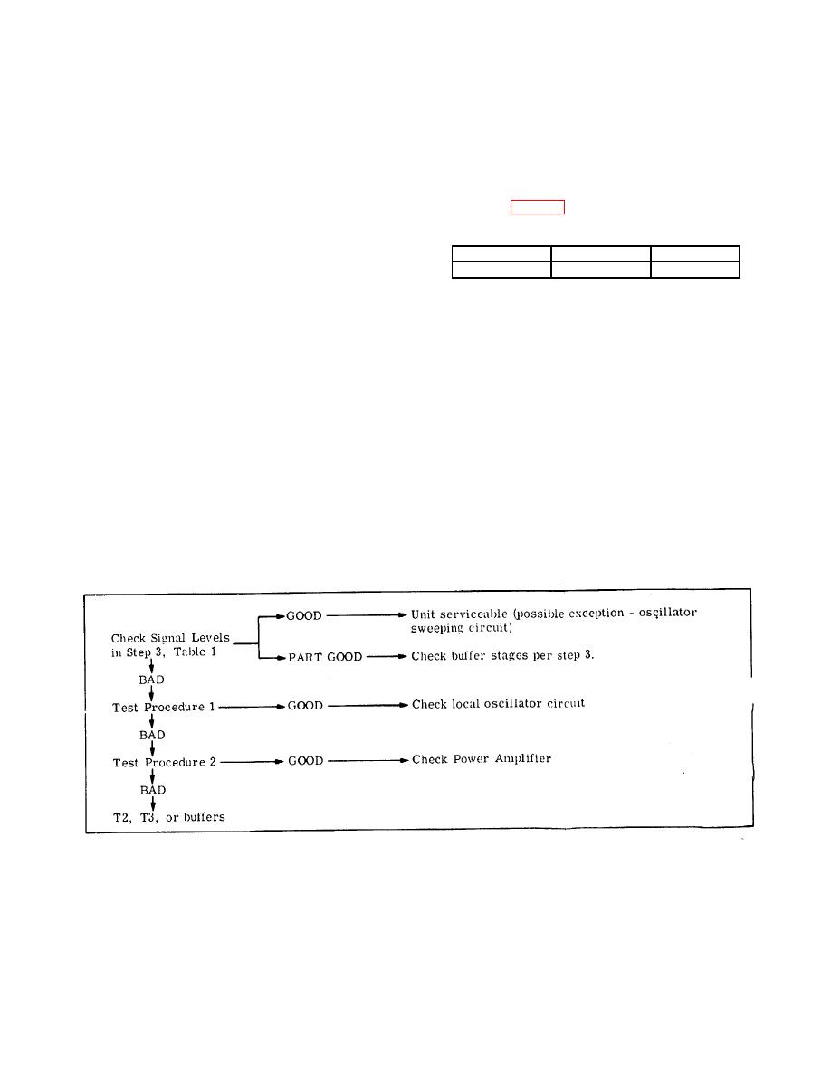
Simplified Test Procedure Tree
