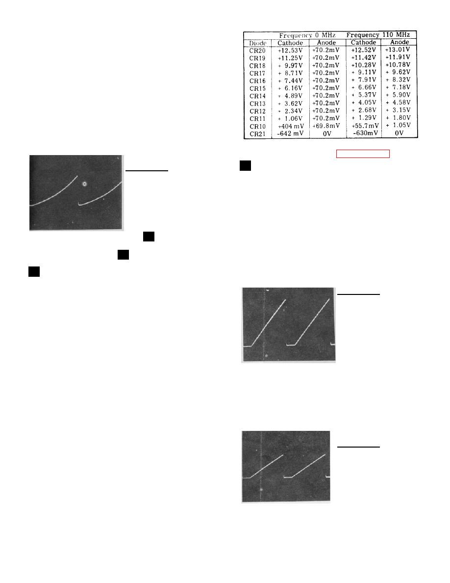
shaping is accomplished by a bias network in the base
circuit of Q4B. The response time of the operational
amplifier is determined by C9 and R23.
TEST PROCEDURES
2-a. Connect Oscilloscope to Test Point D and observe
waveform of 1-c.
CONTROL SETTINGS: Same as 1-a.
Waveform same as 1-c. GOOD: Proceed to step 2-b.
BAD: Check wiring and S2-5F of SCAN WIDTH switch.
After repairing the shaping network it should be
2-b. Connect Oscilloscope to Test Point E and observe
calibrated in accordance with Paragraph 5-22 of Section
waveform shown below.
V. Recheck waveform Test Point E.
4
Oscilloscope:
1 msec/Div
PRESET SCAN AMPLIFIER
1 V/Div
The -5 volt to +5 volt ramp from the Scan Generator
10:1 probe
(A6) is applied to the base of Q1. The ramp is
processed by Q1/Q2 and Q3 to provide a 0 to +12.9 volt
Analyzer:
ramp to the marker generator and the SCAN WIDTH
10 MHz/Div
switch. Offset adjust A4R7 is adjusted to calibrate the
5 msec/Div
marker with respect to the FREQUENCY control.
50 MH4 FREQ.
z
Waveform GOOD: Proceed to step
.
TEST PROCEDURES
Waveform BAD: Check Q2/Q3/Q4 circuits. If trouble is
3
4-a. Connect Oscilloscope to Test Point F and observe
not located proceed to step
.
waveform shown below:
3
SHAPING NETWORK
CONTROL SETTINGS:
Oscilloscope:
Voltage regulation for the shaping network, consisting of
5 msec/Div
resistors R32 through R66, is provided by Q1. Diodes
0.2V/Div
CR10 through CR21 are sequentially forward biased as
10:1 probe
the ramp voltage at the base of Q4 in the shaping
amplifier increases. As each diode is forward biased it
Analyzer:
places additional resistive networks in parallel to reduce
SCAN WIDTH:
the total resistance of the network. When the first local
0-100 MHz
oscillator is being swept from 200 to 310 MHz the ramp
FREQUENCY:
voltage is controlled by the shaping network to provide
50 MHz
the exponential voltage ramp output required to linearly
SCAN TIME
control the first local oscillator frequency. Resistors
2 msec/Div
marked with an asterisk are factory selected values.
Waveform GOOD: Proceed to step 4-b.
Waveform BAD: Input signal not correct or shorted Q1.
TEST PROCEDURES
3-1. Measure voltage at the emitter of Q1. Should be
4-b. Connect Oscilloscope to Test Point G and
+12.5V .1V.
observe waveform.
Voltage GOOD: Proceed to 3-b.
Oscilloscope:
Voltage BAD: Check Q1 circuit.
5 msec/Div
0.5V/Div
3-b. Check biasing network voltages in the following
10:1 probe
chart.
Analyzer:
Same as 4-a.
SERVICE SHEET 7
1 MHz Crystal Oscil., Freq. Divider, & APC
Compensation Circuit
8-38


