
TM 11-6625-2781-14&P-2
a dc error signal and fed back to the first local oscillator
SERVICE SHEET 6
control circuit as a correction signal. When the TUNING
It is assumed that inputs from the VTO and Reference
STABILIZER is in the OFF position, the dc error voltage
assemblies and dc operating voltages are present and
is grounded. Also, on scan widths greater than 20 kHz
correct. It is further assumed that an attempt has been
per division the dc error signal is grounded through the
made to follow the procedures specified in paragraphs
1
scan width attenuator circuit (see Service Sheet 7).
SAMPLER PULSE GENERATOR
A 100 kHz square wave signal derived from the 1 MHz
TROUBLESHOOTING PROCEDURE
crystal oscillator in the Reference Assembly A8 is
When trouble has been isolated to the APC assembly,
applied to coupling capacitor C7. The negative-going
the assembly may be removed from the casting and
portion of the square wave is differentiated by C7 to
reinstalled in an inverted position using the fasteners
produce a negative spike at the base of Q8. The
supplied with the Service Kit to provide easy access to
positive going portion of the square wave is clipped by
all circuit components. Troubleshooting information
CR3. When the negative spikes turn on Q8, the
follows the technical description of the individual
positive-going collector signal is differentiated by C10
circuits.
and R2 and applied to the base of Q7 where negative
NOTE
portions of the signal are clipped by CR7. The negative-
These circuits may be evaluated and
going signal at the collector of Q7 is applied to the
repaired without an input rf signal
primary of T1 to initiate sampler gate pulses by turning
applied to the analyzer. However,
off step-recovery diode CR8.
displaying the 30 MHz calibration
signal on the analyzer display may
Step-recovery diode CR8 is normally biased on. The
be a definite-: aid in evaluating
100 kHz pulses from Q7 are coupled through T1 to both
circuit performance.
ends of the step-recovery diode which is turned off for
one nanosecond by each pulse. The resulting one
EQUIPMENT REQUIRED
nanosecond pulses are applied to both sides of the
Service Kit ................................ ....... HP 11592A
sampler diode quad to turn on all of the diodes
Volt-ohm-ammeter ............................... HP 410C
simultaneously. Resistor R8 is a factory selected
Oscilloscope................... HP 180A/1801A/1821A
component which is selected at final test and assembly
Digital Voltmeter ..................... HP 3440A/3443A
to ensure compatibility with the step-recovery diode and
associated components.
CONTROL SETTINGS
(unless otherwise specified in individual tests.)
TEST PROCEDURE:
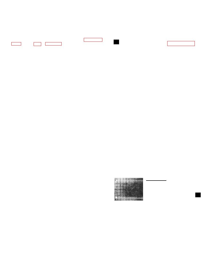
1-a. Connect the HP 180A/1821A Channel A input to TP
SCAN WIDTH PER DIVISION ................ 20 kHz
A, the Channel B input to TP B and observe the
INPUT ATTENUATION . ............................ .0 dB
waveforms.
SCAN WIDTH ............................ PER DIVISION
BANDWIDTH ................................ ............ 3 kHz
CONTROL SETTINGS:
FREQUENCY ................................ ........ 30 MHz
TUNING STABILIZER ................................ ...ON
0.1 /sec/Div
SCAN TIME PER DIVISION.................... 1 msec
0.05 V/Div
LOG REF LEVEL ................................ ..-30 dBm
10:1 probes
LOG REF LEVEL VERNIER................. max ccw
Waveform GOOD: proceed to 2
SCAN MODE . ................................ ............. INT
Waveform BAD: proceed to 1-b.
VIDEO FILTER ................................ ........... OFF
SCAN TRIGGER................................ ...... AUTO
1-b. Connect the HP 180A/1801A/1821A to TP 1 (Q7-c)
and observe the waveform.
AUTOMATIC
PHASE
CONTROL
SAMPLER/AMPLIFIER CIRCUITS (General).
Automatic phase control is initiated when SCAN
WIDTHS of 20 kHz per division or less and TUNING
STABILIZER functions are selected. The first local
oscillator is phase locked (stabilized) to a harmonic of
the 100 kHz reference oscillator. While the analyzer is
phase locked each negative swing of the 100 kHz
reference signal generates a pulse that samples the first
local oscillator output signal. The sample is converted to
