Section VIII
TM 11-6625-2781-14&P-2
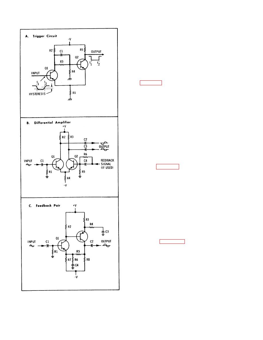
times. The trigger circuit is similar to the flip-flop except
that the RC network in one half is replaced by the input
signal. Capacitor C1 bypasses R3 to couple fast
changes in voltage at the Q1 collector to the base of Q2.
Either Q1 or Q2 can conduct depending on the voltage
at the input. Note that there is a slight difference in
input voltage (called hysteresis) between switching with
a negative-going input (time 1) and switching with a
positive-going input (time 2).
8-24. Differential Amplifier . The differential amplifier
stages coupled together in the emitter circuit. Signals at
the output of the two collectors are 180 degrees out-of-
phase. Inverse feedback may be applied to the base of
Q2 to control gain. As the voltage at the emitter of Q1
changes, the emitter of Q2 also changes by the same
amount. This changes the base-to-emitter bias of Q2.
If a more negative voltage were applied to the base of
Q1, current through Q1 would decrease, causing the
emitter of Q1 to go in the negative direction. A
negative-going voltage at the emitter of Q2 increases
the effective forward bias between base and emitter of
Q2, causing it to conduct more heav ily. Therefore,
when current through Q1 decreases, current through Q2
increases.
8-25. Feedback-Pair Amplifier. The feedback-pair
amplifier (Figure 8-5, Schematic C) is a high-gain direct-
coupled amplifier stage composed of an NPN and a
PNP transistor cascaded together. Feedback for the
pair is accomplished by an RC network between the
collector of Q2 and the emitter of Q1. Voltage gain of
the stage may be calculated by the formula: R5 plus R6
div ided by R6, assuming R7 and R8 are much larger
than R5 and R6. Gain of the amplifier may be
controlled by changing the value of either R5 or R6.
8-26. Flip-Flop . The flip-flop is a bistable two-
transistor circuit in which one transistor conducts,
holding the other cutoff. Each input pulse causes a
reversal of stage; the cutoff transistor is turned on and
the conducting transistor is turned off. In the flip-flop
shown in Figure 8-6, Q1 is conducting heav ily; its
collector voltage is only slightly negative and a near-
zero voltage is supplied to the base of Q2 (R27-R28
junction). The voltage drop across R24 produces a
sufficiently negative voltage at the emitter of Q2 to hold
Q2 cut off. With Q2 cut off, the R18/R19/R20 div ider
delivers a negative volt. age to the base of Q1 to keep it
conducting.
8-27. At time t1 the positive input pulse cuts off Q1; the
Q1 collector voltage goes negative and drives Q2 into
conduction; the Q2 collector voltage and the Q1 base
Figure 8-5. Basic Transistor Circuits.
voltage then become less negative permitting Q1 to
remain cut off. In a similar manner the positive input
produces an output waveform with very fast rise and fall
pulse at time t2 cuts off Q2 and starts a sequence of
8-6


