Section VIII
TM 11-6625-2781-14&P-2
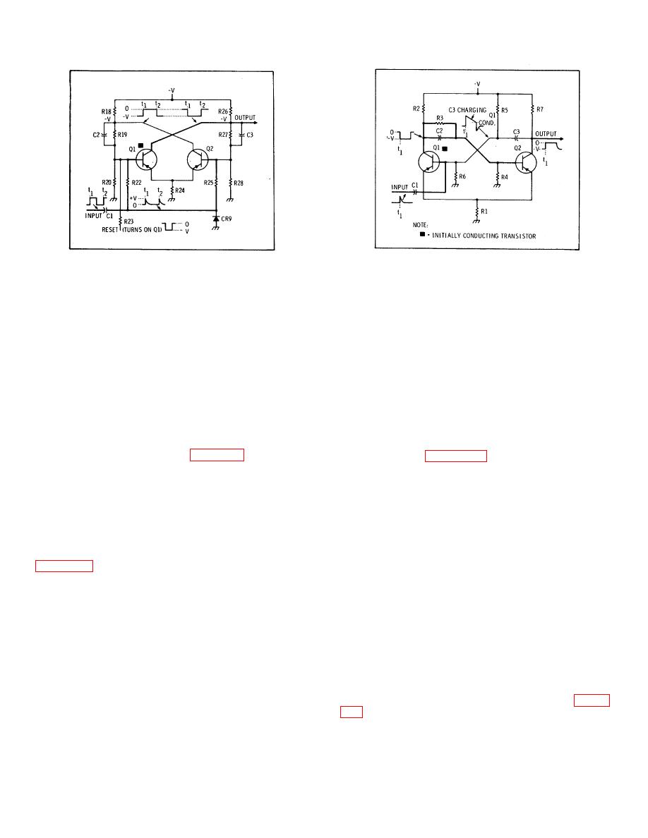
Figure 8-7. Basic One-Shot Multivibrator Circuits.
Figure 8-6. Basic Flip-Flop Circuits.
8-31. Capacitor C3 now charges at a rate mainly
events which ends with Q1 conducting and Q2 cut off.
Note that a positive input pulse has no effect on Q1 if it
determined by the values of R6 and C3 (main charge
is already cut off. A negative reset pulse applied to the
path: R1-Q2-C3-R5). When the Q1 base voltage
base of Q1 returns the flip-flop to its initial condition (Q1
becomes sufficiently negative, Q1 begins conducting.
conducting, Q2 cut off). The diode CR9 removes the
The resulting positive-going Q1 collector voltage is
negative pulse from the differentiated squarewave input.
coupled to the Q2 base, the Q2 collector voltage goes
Without this diode, the negative pulse would drive Q1
negative and is coupled through C3 to the Q1 base to
which is cut off, and the stage would switch from one
further increase Q1 conduction.
The process is
state to the other but would not div ide by two. The ac
regenerative and ends with the circuit in its original
coupling through C2 and C3 insures fast switching. The
quiescent state: Q1 saturated and Q2 cut off, until the
dc coupling through R19 and R27 insures bistable
next pulse is received.
characteristics.
transistors (see Figure 8-8) have three terminals;
shot multiv ibrator is a circuit which generates a pulse of
source, drain, and gate, which correspond in function to
some specified duration following the application of a
emitter, collector, and base of junction transistors.
suitable triggering pulse. The circuit is similar to the flip-
Source and drain leads are attached to the same block
flop except one dc coupling path has been removed so
(channel) of N or P semiconductor material. A band of
the circuit is stable only in the state in which Q1
oppositely doped material around the channel (between
conducts.
the source and drain leads) is connected to the gate
lead.
8-29. In the typical one-shot multiv ibrator shown in
initial stable period: the R5-R6 div ider prov ides a
reverse-biases the PN junction, causing an electric field
smaller negative voltage to the base of Q2 to hold Q2
that creates a depletion region in the source-drain
off.
channel. In the depletion region the number of available
current carriers is reduced as the reverse biasing
voltage increases, making source-drain current a
8-30. The positive triggering pulse at time t1 reduces
function of gate-source voltage. With the input (gate-
conduction of Q1. The resulting negative-going voltage
source) circuit reverse-biased, the FET presents a high
at the collector of Q1 is applied to the Q2 base through
impedance to its signal sources (as compared with the
the R3-R4 div ider (C2 bypasses R3 to prov ide coupling
low impedance of the forward-biased junction transistor
for the rapidly changing voltage at the Q1 collector); Q2
base-emitter circuit). Because there is no input current,
begins to conduct; the resulting positive-going change in
FET's have less noise than junction transistors. Figure
Q2 collector voltage is coupled through C3 to the base
of Q1 to further decrease Q1 conduction. The process
channel and P channel field effect transistors.
is regenerative and quickly results in Q1 being cut off
and Q2 being saturated.
8-7


